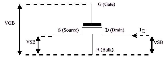
Fig. 1. The n- MOS Transistor Symbol
Although much is known and published on the MOS device subject, for example Operation and modeling of the MOS Transistor by Yannis P. Tsividis one could consider to be the BIBLE, it seems that it is difficult to get a simple model one can use for hand calculation and gives fast answers to questions like: if I have 1uA how big should my MOST be to be in moderate inversion, or For a current mirror to have a 5 to 10% error, how big must my MOST be, or even more terrifying: how big should the transistors be in a differential pair to get 5mV DC offset ?
The model presented below has successfully been used by the author for the last 10 years and it seems that although some companies has 50 models implemented in different CAD programs and technologies, this model is pretty accurate and extremely handy for hand calculations for everybody to use.
In the following some explanation is given, so that one understands
the limits and the simplifications used. The summary shows the important
equations on one page. Print this page to have
them always handy.
Fig. 1. The n- MOS Transistor Symbol
As a general comment I would like to state that the drain and source are defined by the direction of the current flow. This means that per definition holds: Vds > 0 V. (for a p- MOS: Vds < 0V) Although there is no physical difference between source and drain, some like to develop models that allow the terms source and drain to be interchangeable by defining all voltages against the bulk. It is the author's opinion that the models that result out of this perfectionism are hard to use for hand calculations and make it highly unlikely that by using them designers get a good feeling on how a circuit works.
The model that is described here, describes only an n- MOS and is based
on the model developed J. Fellrath and by E. Vittoz and in the mid seventies
- yup, that's 25 years ago
- . They have shown that holds for the weak
inversion region:( see fig. 1. for voltage and current definitions)
with U T =KT/ q ~ 25mV at room temperature.
The condition for a transistor working in strong or weak inversion will be given later. For now it is enough to know that the transistor's current density is low. I use as a rule of thumb:
A 200u/ 1u transistor drawing less then 1uA is in weak inversion
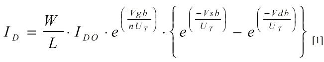
Equation [1] looks pretty complicated to me and I won't use it for hand calculation, however, for getting an idea, one can simplify equation [1] a bit when the source is connected to the bulk, which happens quite often, then [1] converts into:
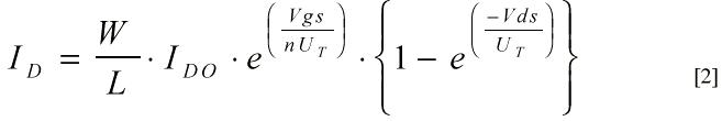
This looks still to complicated. Since normally Vds>> 125mV
-Ive never seen a MOS switch in weak inversion- one can simplify to :
The equation [3] looks pretty much like the one for the bipolar transistor. This also shows that the current is pretty difficult to control by the Vgs voltage, however, the Vgs is easy to control by the current. Actually, the IDO term is of no practical use, since it can vary decades from batch to batch. [3] is only of interest for determining the transconductance of the device. With equation [3] one can understand already now (equations will be derived later) that:
1) Weak inversion current mirrors have a high current mismatch.
2) Weak inversion differential pairs have a low input referred voltage
offset
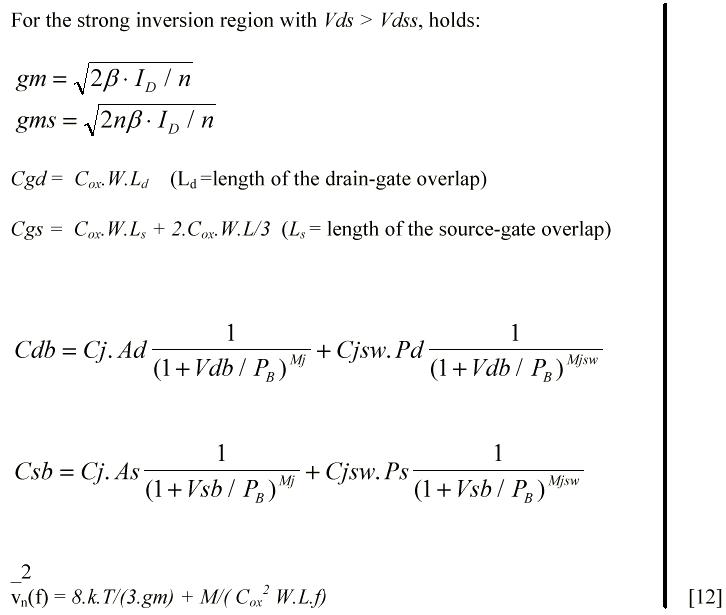
For strong inversion (the condition for this region will be described later too) one can derive:
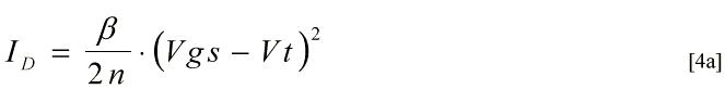
for Vds >Vdss (Most in saturation)
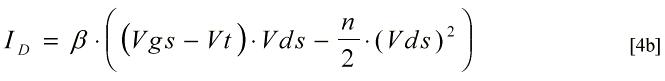
for Vds< Vdss (Most in linear region, a switch in the on state for example)
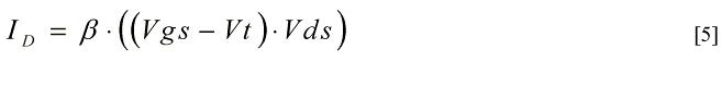
These equations look simple enough. For hand calculation the expression [4b] for linear region can be simplified further, since most of the time holds Vds<< Vgs- Vt.
As interesting intermezzo one can state that there is even an approximate expression known that describes all regions (weak inversion, strong inversion and in between) pretty accurately. Unfortunately this expression is too complicated for hand calculation and therefore not given here.
To complete the equations above, one can add:
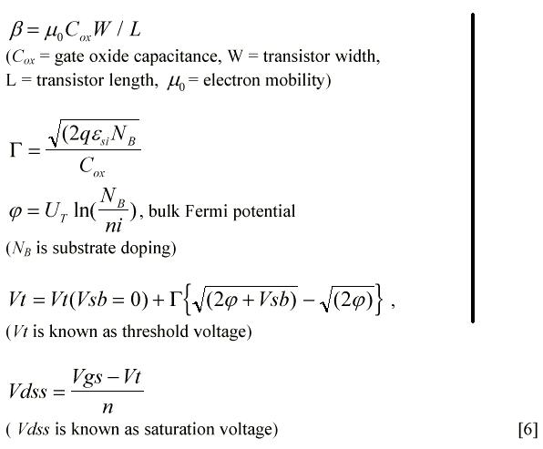
Also, in the formulas above, n is introduced: (also known as weak inversion slope factor)
![]()
[7] can be simplified if one assumes the number of fast surface states (Nfs)
![]()
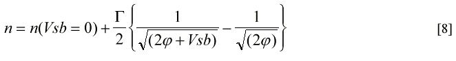
Since the depletion capacitance Cd depends on Vsb, the weak inversion slope factor depends on the source to substrate voltage Let n0 be the slope factor at Vsb = 0 V, one can derive:
Since in modern technologies, the gate- oxide densities are pretty high because of the decreasing oxide thickness:
![]()
This results n to pretty low. n0 is in the range of 1.3~ 1.2 and in [8] the second term can be neglected:
![]()
A good starting point for determining n -which is not really a SPICE
parameter for a technology is using ![]() (sometimes
called KP):
(sometimes
called KP):
![]()
Now the expression for the threshold voltage in [6] can be simplified to (see also fig. 2):
![]()
Figure 2. The approximation equation for the threshold voltage
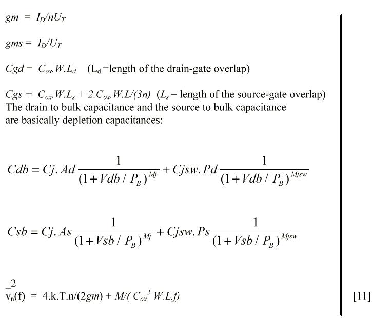
Now that most of the DC currents and voltage relation ships are known
one can now proceed to write down the small signal parameters (See fig.
3 for the definitions)

Figure 3. The small signal model
! Note that the generator gm is not the same as in a lot of text-books ("Analysis and Design of Analog Integrated Circuits," Paul Gray and Robert Meyer) and even in most programs like SPICE ("Semiconductor Device Modeling with SPICE," Paolo Antognetti and Guiseppe Massobrio), where the controlling node for the gm current source is Vgs. For the practical case where the source is connected to the bulk they are equivalent and gms = 0
For the MOST working in the weak inversion region with
Vds > 125mV (5UT) one can derive:
! Note: The parameters
in the equations above are SPICE parameters and are directly available
the SPICE model that you use.
The second term in the equation for the equivalent input noise voltage
source is the flicker noise component. M is obviously technology dependent,
however, for most technologies the frequency is given where the flicker
noise contribution equals the thermal noise contribution. Depending on
a certain bias, one can then easily determine M with [11] and [12]. It
is also interesting to notice that the flicker noise component has a tendency
to improve with technology scaling.
If M is not available, one can use the values:
The channel length modulation can be modeled with gds. In weak and strong inversion one can use the handy first order approximation (see Fig. 3):
![]()
Sometimes it is hard to get the right Vearly voltage, because it probably doesnt exist in the SPICE model that is used. However, for a first approximation one can use:
![]()
! Note: The equation above takes oxide scaling into account. However, for very small channel lengths, the accuracy might be compromised. One should verify the accuracy of [14] for the process used by sweeping Vds in SPICE.
For the moderate inversion region (my favorite region of operation for a MOS, since it gives best of both worlds) handy equations can also be derived:
First, an IDlim is introduced:

Assume the transistor to work in weak inversion if holds:
![]()
and assume the transistor to work in strong inversion if holds:
![]()
Then, if UPLIM and DOWNLIM > 8, the small signal equations [11] and
[12] are valid.
If [15] and [16] do not hold with DOWNLIM and UPLIM >8 a LIM value
can always be found. Define:
![]()
After having determined the LIM value for a transistor and LIM is in
between 1/ 8 and 8, the following approximations can be used:

Interesting to note is that The first part of equation [19] converts
into the expression for gm described in [12] if LIM is large and to the
expression for gm described in [11] when LIM is small. The expression gm
described in [19] can be considered to be a handy interpolation function
.
Last, but not least, some simple equations for current and gate voltage MISMATCH can be derived by taking the right derivatives of the previous equations:
With
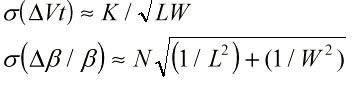
follows the gate voltage mismatch of a differential pair:
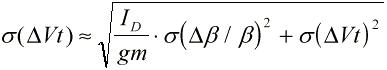
and the current mismatch of a current mirror:

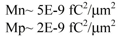
The threshold voltage and beta mismatch (sigma value) should be available for a given technology, however, if they are not one can use the following for a first order approximation:
Kn ~ 16 mV. um
Kp ~ 31 mV. um
Nn ~ 1.6E-2 um
Np ~ 2.4E-3 um
(The index n or p indicate a NMOS or a PMOS)
An interesting approach is to see the threshold voltage offset as if
it equals the flicker noise component where f goes to 0. Although ![]() doesnt equal
doesnt equal ![]() , it does indicate that the offset voltage reduces with decreasing oxide
thickness. I havent put a lot of thought into this, but it wouldnt surprise
me to be correct: As Cox increases, n decreases and the equations for the
MOS in weak inversion start to look like the equations for a bipolar device
(n=1). Why wouldnt the flicker noise and the offset voltage decrease as
well ?
, it does indicate that the offset voltage reduces with decreasing oxide
thickness. I havent put a lot of thought into this, but it wouldnt surprise
me to be correct: As Cox increases, n decreases and the equations for the
MOS in weak inversion start to look like the equations for a bipolar device
(n=1). Why wouldnt the flicker noise and the offset voltage decrease as
well ?
Copyright © 1999 by Matthijs Pardoen
![]() "A
Simple and Pretty Accurate MOS Model for Hand Calculations -Equation Summary-",
Matthijs Pardoen, May 1999
"A
Simple and Pretty Accurate MOS Model for Hand Calculations -Equation Summary-",
Matthijs Pardoen, May 1999